
Blog
The Machine Behind Your RAM, and Why It Matters for the AI Tools Your Team Builds
Inspired by Veritasium's video "The Closest Thing We Have to Alien Technology".
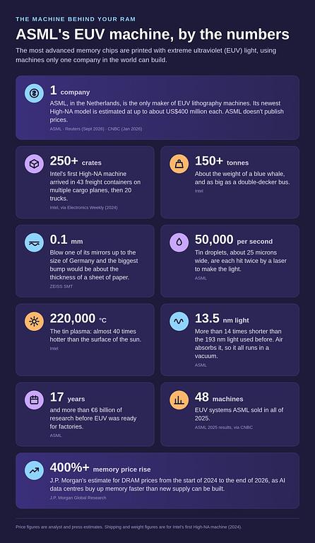
There's a RAM shortage, and plenty of people are blaming AI. They're not wrong. AI data centres are buying memory as fast as it can be made, and J.P. Morgan expects DRAM prices to rise more than 400% between the start of 2024 and the end of 2026.
But look a little deeper and there's a harder question: why can't memory makers just build more? Part of the answer is that the most advanced memory made today depends on a machine that only one company in the world can build. The newest model is estimated to cost up to about US$400 million. Intel's first High-NA machine arrived in more than 250 crates, packed into 43 freight containers and flown in on several cargo planes. Inside are mirrors so smooth that if you blew one up to the size of Germany, the biggest bump would be about a tenth of a millimetre, roughly the thickness of a sheet of paper.
That company is ASML, based in the Netherlands. ASML doesn't make memory, or chips of any kind. It builds the lithography machines that chipmakers use to print patterns onto silicon. Memory makers such as Samsung, SK hynix and Micron use those machines to produce their most advanced DDR5.
If your team is building its own AI tools, this matters more than it sounds. Memory is one of the quiet limits on what those tools can do and where they can run.
What "printing" a chip means
A memory chip is built up in layers on a silicon wafer. Each layer starts as a pattern of billions of tiny lines and holes. Lithography transfers that pattern. Light reflects off or passes through a template called a mask, optics shrink the image, and it lands on a wafer coated in light-sensitive material. The wafer is then etched or treated, and the cycle repeats for the next layer.
The rule of thumb is simple. In ASML's words: "The shorter the wavelength of light, the smaller the microchip features that can be printed."
From deep ultraviolet to extreme ultraviolet
For years the industry's workhorse was deep ultraviolet (DUV) lithography, at a wavelength of 193 nanometres. Chipmakers stretched it by exposing the same layer several times, and every extra pass adds cost, time and chances for defects.
Extreme ultraviolet (EUV) lithography uses light at 13.5 nanometres, which ASML describes as "more than 14 times shorter" than DUV. ASML is the only company that makes EUV systems.
Making that light is the part that earns the "alien technology" label. In ASML's description, droplets of molten tin about 25 microns across fall through the machine at 70 metres per second. One laser pulse flattens each droplet, and a second, stronger pulse turns it into a plasma that gives off EUV light. This happens 50,000 times a second. EUV light is absorbed by almost everything, including air, so the whole process runs in a vacuum and uses mirrors instead of lenses.
EUV still hasn't replaced DUV. ASML says EUV handles "the most intricate layers on a chip," and DUV machines still print the rest.
Where EUV entered memory
- Samsung began mass-producing 14 nm DRAM for DDR5 with five EUV layers in October 2021. It said that node wasn't possible with the older argon fluoride process.
- SK hynix started using EUV in mass production in July 2021. In August 2024 it announced the industry's first 16 Gb DDR5 on its sixth-generation "1c" node.
- Micron waited longer. Its first EUV node, "1γ" (1-gamma), began sampling as DDR5 in February 2025.
Labels like "1c" and "1γ" are generation names within the "10 nm class", not exact measurements, so they can't be compared directly across companies.
The DDR5 standard, published by JEDEC in 2020, doesn't say how chips must be made. In practice, though, fitting more bits onto each chip at higher speeds and lower power is what pushed memory makers onto EUV for their most advanced parts.
What's next, and why it's a bottleneck
ASML's newest machines, called High-NA EUV, use larger optics to print even finer detail. In September 2025, SK hynix announced it had assembled the industry's first High-NA system for mass production, at its fab in Icheon, South Korea, to help develop next-generation DRAM. What that means for memory after DDR5 isn't public yet, and we won't guess.
These machines cost hundreds of millions of dollars each, and there's only one supplier. The number of them a memory maker can get and keep running puts a real limit on how quickly new memory reaches the market.
Why this matters if your team builds its own AI tools
Memory is often what decides whether a tool your team builds can run on hardware you control, or has to send your data somewhere else. AI models need to hold a lot of data close to the processor while they work. When memory is scarce or expensive, the easy answer is to send everything to someone else's cloud. As memory gets denser and cheaper, more of that work becomes practical closer to home.
You don't need to understand lithography to plan well. But when you're deciding what's worth building now and what's worth waiting for, it helps to know that the hardware underneath is still moving. Some of today's trade-offs between cost, speed and keeping your data in-house may look different as newer memory reaches the market.
Sources
- ASML, "All about light and lasers in lithography". https://www.asml.com/en/technology/lithography-principles/light-and-lasers
- ASML, "EUV lithography systems". https://www.asml.com/en/products/euv-lithography-systems
- Samsung Newsroom, "Samsung Starts Mass Production of Most Advanced 14nm EUV DDR5 DRAM" (12 Oct 2021). https://news.samsung.com/global/samsung-starts-mass-production-of-most-advanced-14nm-euv-ddr5-dram
- SK hynix Newsroom, "SK hynix Starts Mass Production of 1anm DRAM Using EUV Equipment" (12 Jul 2021). https://news.skhynix.com/en/sk-hynix-starts-mass-production-of-1anm-dram-using-euv-equipment/
- SK hynix Newsroom, "SK hynix Develops Industry's First 1c DDR5" (29 Aug 2024). https://news.skhynix.com/en/sk-hynix-develops-industry-first-1c-ddr5/
- SK hynix Newsroom, "SK hynix Introduces Industry's First Commercial High NA EUV" (3 Sep 2025). https://news.skhynix.com/en/sk-hynix-introduces-industrys-first-commercial-high-na-euv/
- Micron, "Micron Announces Shipment of 1γ (1-gamma) DRAM" (25 Feb 2025). investors.micron.com; Micron 1γ technology page. https://www.micron.com/products/memory/1gamma-dram-technology
- JEDEC, "JEDEC Publishes New DDR5 Standard…" (14 Jul 2020). https://www.jedec.org/news/pressreleases/jedec-publishes-new-ddr5-standard-advancing-next-generation-high-performance
- Reuters, "ASML's next chip challenge: rollout of its new High NA EUV machine" (9 Feb 2024). https://www.reuters.com/technology/asmls-next-chip-challenge-rollout-its-new-350-mln-high-na-euv-machine-2024-02-09/
- J.P. Morgan Global Research, "The AI-Driven Memory Shortage: DRAM Prices, Inflation and Market Risks" (2026). https://www.jpmorgan.com/insights/global-research/artificial-intelligence/dram-memory-shortage-from-ai
- Reuters, "ASML extends chipmaking dominance as customers embrace High NA" (14 Sep 2026). https://www.reuters.com/world/asia-pacific/asml-extends-chipmaking-dominance-customers-embrace-high-na-2026-09-14/
- CNBC, "Why Nvidia's AI boom couldn't happen without Dutch chip equipment maker ASML" (29 Jan 2026). https://www.cnbc.com/2026/01/29/-ai-boom-nvidia-asml-dutch-chip-equipment-maker-lithography-.html
- Intel Newsroom, "High NA EUV at Intel". https://www.intel.com/content/www/us/en/newsroom/resources/intel-high-na-euv.html
- Electronics Weekly, "Intel moving second High NA EUV tool into Oregon" (Aug 2024). https://www.electronicsweekly.com/news/business/intel-moving-second-high-na-euv-tool-into-oregon-2024-08/
- ZEISS SMT, "EUV lithography". https://www.zeiss.com/semiconductor-manufacturing-technology/inspiring-technology/euv-lithography.html